
Semiconductor
High-precision 3D visual inspection solution meeting stringent semiconductor industry standards
Industry Pain Points
Small, high-precision components with stringent manufacturing requirements.

Semiconductor packaging demands extreme precision; micron-level defects are unacceptable.

Challenging to inspect processes such as wire bonding and die attach.

Cleanroom requirements: Equipment must be compatible with cleanroom conditions.
Solutions
Semiconductor Visual Inspection Solution
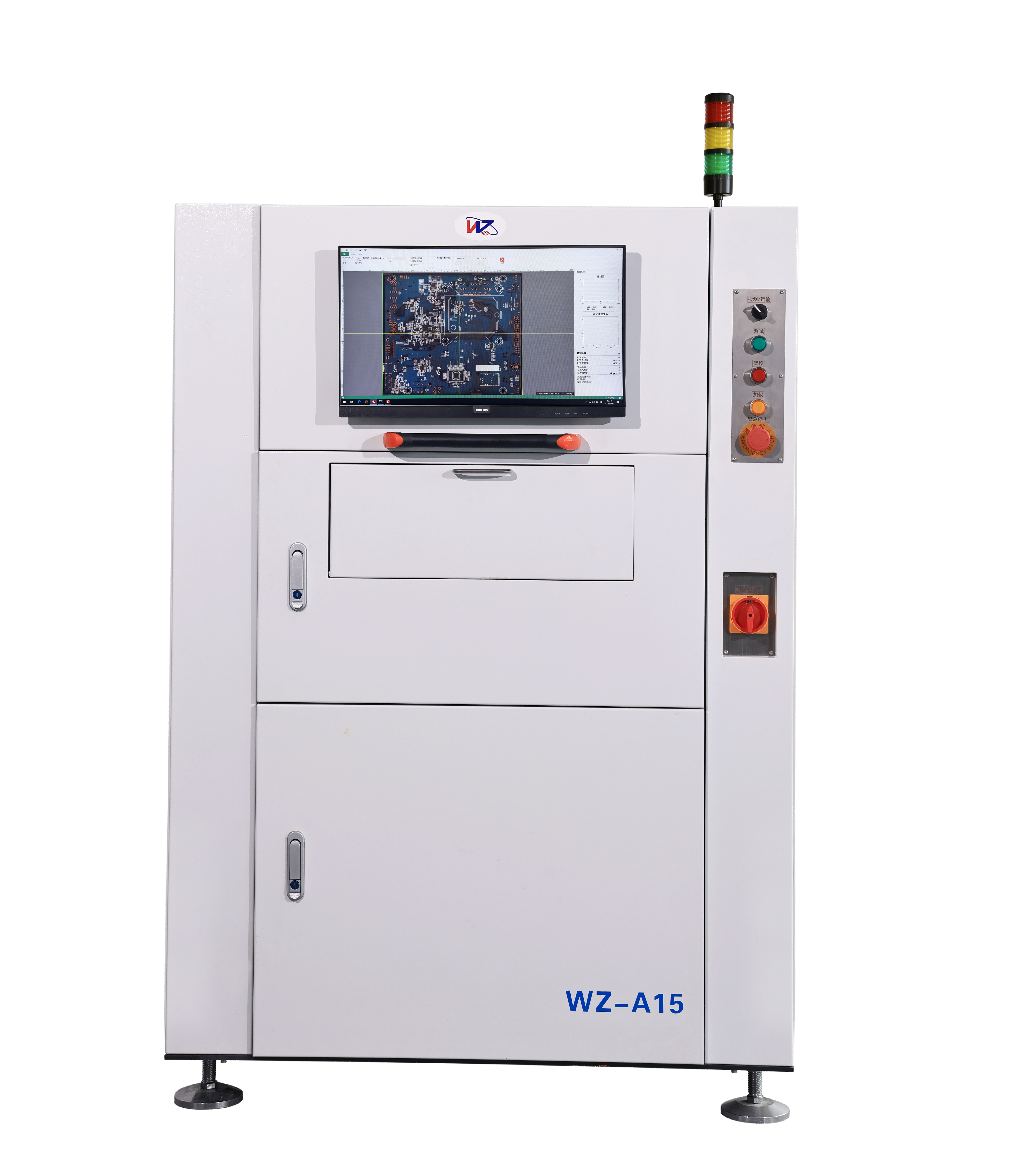
WZ-3D AOI
High-precision detection
High-resolution camera combined with sub-pixel algorithms meets the high-precision inspection requirements of semiconductor packaging.
3D Topography Analysis
Multi-angle structured light projection for precise 3D reconstruction of solder joints and packages, enabling detection of coplanarity, warpage, and other critical metrics.
Clean Adaptation
Designed for cleanroom environments with low dust and vibration, optimized for semiconductor manufacturing processes.
Solution Benefits
forSemiconductorMore reliable security

Supports 01005 ultra-small component inspection, meeting high-precision detection requirements for micro-devices in semiconductor packaging.

3D solder joint inspection capability to identify various welding defects.

Self-developed neural network algorithms continuously optimize detection models to effectively reduce false positives and minimize manual review.

Full-process data traceability with MES integration for closed-loop quality management.